Thermal control of a storage device receiving a limited amount of power
Summary by NHIP
Power-Limited Storage Thermal Control
The electronic device manages heat in a power-constrained storage unit by coordinating a thermal reduction device with a power savings mode. The thermal control unit activates the cooling device only when the storage unit consumes reduced power sufficient to meet a maximum average power threshold, whereas deactivation occurs when power consumption is insufficient to operate the thermal reduction device.
Claim Score by NHIP
Abstract
An electronic device including a thermal reduction device, and a storage device electrically connected to the thermal reduction device. The storage device including a media, a channel configured to perform data operations on the media, a power input interface configured to receive power for consumption by the storage device from an available average amount of power, wherein the received power reduces the available average amount of power, and the available average amount of power is no greater than a maximum average power threshold, a thermal sensor configured to generate thermal data corresponding to a temperature of the storage device, and a thermal control unit configured to activate or deactivate a power savings mode for the storage device based at least on the thermal data, and to activate or deactivate the thermal reduction device based at least on the thermal data. The power savings mode affects an operation of the channel.
Term
7.4 yearsleft in the term
Expires 1 February 2034, including 324 days of term adjustment.
- Priority and filed
- Granted
- Today
- Expires
20 claims: 3 independent, 17 dependent
- 1An electronic device comprising:a thermal reduction device;and a storage device electrically connected to the thermal reduction device comprising: a media;a channel configured to perform data operations on the media;a power input interface configured to receive power for consumption by the storage device from an available average amount of power, wherein the received power reduces the available average amount of power, and the available average amount of power is no greater than a maximum average power threshold;a thermal sensor configured to generate thermal data corresponding to a temperature of the storage device;and a thermal control unit configured to activate or deactivate a power savings mode for the storage device based at least on the thermal data, and to activate or deactivate the thermal reduction device based at least on the thermal data, wherein the power savings mode affects an operation of the channel, when the power savings mode is deactivated, the storage device is configured to consume an average amount of power such that the available average amount of power is insufficient to operate the thermal reduction device, and when the power savings mode is activated, the storage device is configured to consume a reduced average amount of power such that the available average amount of power is sufficient to operate the thermal reduction device;wherein the storage device is configured to consume a first average amount of power when the power savings mode is deactivated and to consume a second average amount of power when the power savings mode is activated, wherein the second average amount of power is less than the first average amount of power.
- 10Broadest claimClaim Score 37, narrow(NHIP)A method for operating an electronic device comprising a thermal reduction device and a storage device electrically connected to a thermal reduction device, the method comprising at least:receiving power for consumption by the storage device from an available average amount of power, wherein the received power reduces the available average amount of power, and the available average amount of power is no greater than a maximum average power threshold;generating thermal data corresponding to a temperature of the storage device;activating or deactivating a power savings mode for the storage device based at least on the thermal data, wherein the power savings mode affects an operation of a channel in the storage device;when the power savings mode is deactivated, consuming an average amount of power in the storage device such that the available average amount of power is insufficient to operate the thermal reduction device;when the power savings mode is activated, consuming a reduced average amount of power in the storage device such that the available average amount of power is sufficient to operate the thermal reduction device;activating or deactivating the thermal reduction device based at least on the thermal data;when the power savings mode is deactivated, consuming a first average amount of power in the storage device;and when the power savings mode is activated, consuming a second average amount of power in the storage device, wherein the second average amount of power is less than the first average amount of power.
- 19A storage device configured to electrically connect to a thermal reduction device comprising:a media;a thermal sensor configured to generate thermal data corresponding to a temperature of the storage device;a thermal control unit configured to activate or deactivate a power savings mode for the storage device based at least on the thermal data, and to activate or deactivate the thermal reduction device based at least on the thermal data, when the power savings mode is deactivated, the storage device is configured to consume an average amount of power such that an available average amount of power is insufficient to operate the thermal reduction device, and when the power savings mode is activated, the storage device is configured to consume a reduced average amount of power such that the available average amount of power is sufficient to operate the thermal reduction device;and a channel configured to perform data operations on the media, wherein when the power savings mode is deactivated, the channel is configured to perform a first average amount of data operations on the media, and when the power savings mode is activated, the channel is configured to perform a second average amount of data operations on the media, wherein the second average amount of data operations is less than the first average amount of data operations, and the second average amount of data operations is based on an average amount of power consumed by the thermal reduction device.
Independent claims3
42 paragraphs in 3 sections, as filed
BACKGROUND
In a conventional disk drive, the conventional disk drive may become damaged if the temperature of the conventional disk drive is too high for too long of a period. Thus, the conventional disk drive may monitor the temperature of the conventional disk drive and implement cooling measures to reduce the temperature of the conventional disk drive when the conventional disk drive determines that the temperature of the conventional disk drive is too high. However, such cooling measures generally require a large amount of time to reduce the temperature of the conventional disk drive. In addition, the cooling measures typically reduce a performance of the conventional disk drive. Thus, the conventional disk drive may have a reduced performance for a large amount of time when the cooling measure is implemented to reduce the temperature of the conventional disk drive.
The conventional disk drive may also be cooled by a fan in a conventional computer. However, the fan is controlled by another device aside from the conventional disk drive. The device may turn on the fan when the fan is not needed to cool the conventional disk drive. Furthermore, the device may not turn on the fan fast enough to cool the conventional disk drive. Thus, the conventional disk drive may not be appropriately cooled by the fan. In addition, the fan generally draws additional power, which may increase a power consumption of the conventional computer. The increased power consumption of the conventional computer may be undesirable.
BRIEF DESCRIPTION OF THE DRAWINGS
The features and advantages of the present embodiments will become more apparent from the detailed description set forth below when taken in conjunction with the drawings, wherein:
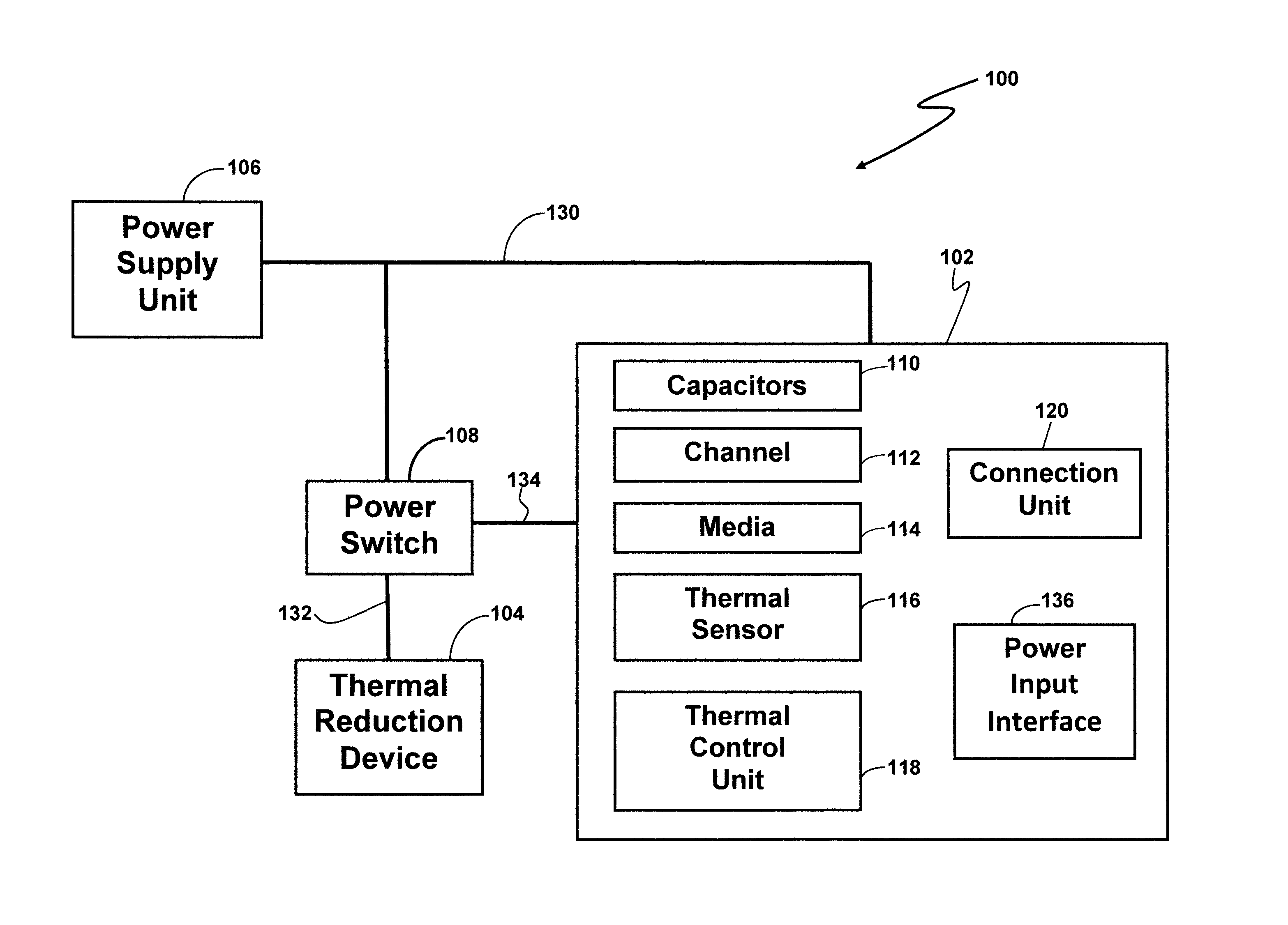
<figref idref="DRAWINGS">FIG. 1</figref> is a box diagram of an electronic device comprising a storage device and a thermal reduction device according to an embodiment;
<figref idref="DRAWINGS">FIG. 2</figref> depicts a graph indicating thermal data, and a graph indicating average power consumption of a storage device and average power consumption of a thermal reduction device, according to an embodiment; and
<figref idref="DRAWINGS">FIG. 3</figref> depicts a process for operating an electronic device comprising a thermal reduction device and a storage device according to an embodiment.
DETAILED DESCRIPTION
In an embodiment shown in <figref idref="DRAWINGS">FIG. 1</figref>, an electronic device <b>100</b> comprises a storage device <b>102</b>, a thermal reduction device <b>104</b>, a power supply unit <b>106</b>, and a power switch <b>108</b>. In an embodiment, the electronic device <b>100</b> comprises a computer, a laptop, a tablet, a media streaming unit, a set top box, a watch, or other device which utilizes a storage device <b>102</b> which needs to be cooled. In an embodiment, the power supply unit <b>106</b> supplies a limited average amount of power to the storage device <b>102</b> and the thermal reduction device <b>104</b>. In an embodiment, the storage device <b>102</b> is electrically connected to the thermal reduction device <b>104</b>.
In an embodiment, the limited average amount of power comprises an available average amount of power for the storage device <b>102</b> and the thermal reduction device <b>104</b>. That is, when the storage device <b>102</b> consumes power, it reduces the available average amount of power such that there is less power available for the thermal reduction device <b>104</b>. Similarly, when the thermal reduction device <b>104</b> consumes power, it reduces the available average amount of power such that there is less power available for the storage device <b>102</b>. In an embodiment, the available average amount of power is no greater than a maximum average power threshold.
In an embodiment, the storage device <b>102</b> is configured to activate or deactivate the thermal reduction device <b>104</b>, which will be described in more detail below.
In an embodiment, the storage device <b>102</b> comprises capacitors <b>110</b>, a channel <b>112</b>, a media <b>114</b>, a thermal sensor <b>116</b>, a thermal control unit <b>118</b>, a connection unit <b>120</b>, and a power input interface <b>136</b>. In an embodiment, the storage device <b>102</b> receives power from the power input interface <b>136</b>. The power input interface <b>136</b> can, for example, be configured to receive power for consumption by the storage device <b>102</b> from the available average amount of power supplied by the power supply unit <b>106</b>. In an embodiment, the power input interface <b>136</b> receives power from the power supply unit <b>106</b> using a power line <b>130</b>. In an embodiment, the capacitors <b>110</b> are configured to reduce peak power usage by the storage device <b>102</b> and can be connected to the power input interface <b>136</b>.
For example, the storage device <b>102</b> may utilize instant power that may oscillate, or rapidly increase or decrease even when the average amount of power used by the storage device <b>102</b> remains relatively constant. The capacitors <b>110</b> can act as a reservoir of power such that when the storage device <b>102</b> suddenly requires a large amount of instant power for a short period of time, the capacitors <b>110</b> can supply some or all of the power to the storage device <b>102</b>. This can smooth out the instant power drawn by the storage device <b>102</b> from the power supply unit <b>106</b> as the capacitors <b>110</b> can be recharged at different times or even for a longer period of time. For example, the capacitors <b>110</b> can be charged when the storage device <b>102</b> suddenly requires a low amount of instant power for a short period of time. Thus, the instant power drawn by the storage device <b>102</b> from the power supply unit <b>106</b> can be closer to the average amount of power used by the storage device <b>102</b>, which reduces the peak power usage by the storage device <b>102</b>.
In an embodiment, the channel <b>112</b> is configured to perform data operations on the media <b>114</b>. In an embodiment, the data operations comprises read or write operations. In an embodiment, the media <b>114</b> comprises a magnetic rotating disk. In an embodiment, the media <b>114</b> comprises a solid state memory. In an embodiment, the media <b>114</b> comprises at least one of a magnetic rotating disk and a solid state memory. In an embodiment, the media <b>114</b> comprises both the magnetic rotating disk and the solid state memory.
While the description herein refers to solid state memory generally, it is understood that solid state memory may comprise one or more of various types of solid state non-volatile memory devices such as flash integrated circuits, Chalcogenide RAM (C-RAM), Phase Change Memory (PC-RAM or PRAM), Programmable Metallization Cell RAM (PMC-RAM or PMCm), Ovonic Unified Memory (OUM), Resistance RAM (RRAM), NAND memory (e.g., single-level cell (SLC) memory, multi-level cell (MLC) memory, or any combination thereof), NOR memory, EEPROM, Ferroelectric Memory (FeRAM), Magnetoresistive RAM (MRAM), other discrete NVM (non-volatile memory) chips, or any combination thereof.
The thermal sensor <b>116</b> can, for example, be configured to generate thermal data corresponding to a temperature of the storage device <b>102</b>. In an embodiment, the thermal sensor <b>116</b> comprises a thermometer. In an embodiment, the thermal control unit <b>118</b> is configured to receive the thermal data from the thermal sensor <b>116</b>. The thermal control unit <b>118</b> can, for example, be configured to control operations of the storage device <b>102</b> and the thermal reduction device <b>104</b> based on the thermal data. In an embodiment, the thermal control unit <b>118</b> is configured to activate the power savings mode and the thermal reduction device <b>104</b> in order to reduce the temperature of the storage device <b>102</b> and prevent the storage device <b>102</b> from overheating.
For example, in an embodiment, the thermal control unit <b>118</b> is configured activate or deactivate a power savings mode for the storage device <b>102</b> based at least on the thermal data, which will be described in more detail below. In an embodiment, the power savings mode reduces average power consumption of the storage device <b>102</b> in order to reduce a temperature of the storage device <b>102</b>.
In an embodiment, the power savings mode reduces average power consumption of the storage device <b>102</b> by affecting an operation of the channel <b>112</b>. For example, when the power savings mode is deactivated, the channel <b>112</b> is configured to perform a first average amount of data operations on the media <b>114</b>. However, when the power savings mode is activated, the channel <b>112</b> is configured to perform a second average amount of data operations on the media <b>114</b>. In an embodiment, the second average amount of data operations is less than the first average amount of data operations. In an embodiment, the reduction in average amount of data operations performed by the channel <b>112</b> on the media <b>114</b> reduces average power consumption by the storage device <b>102</b>.
In an embodiment, the second average amount of data operations is based on an average amount of power consumed by the thermal reduction device <b>104</b>. For example, the channel <b>112</b> can be configured to reduce the average amount of data operations on the media <b>114</b>, and reduce power consumption of the storage device <b>102</b> such that the available amount of power is sufficient to power the thermal reduction device <b>104</b>.
In an embodiment, the reduction in average amount of data operations performed by the channel <b>112</b> can be based on a type of the media <b>114</b>. For example, the channel <b>112</b> can be configured to skip revolutions of the media <b>114</b> during a write operation when the media <b>114</b> is a magnetic rotating disk. Similarly, the channel <b>112</b> can be configured to reduce a data write rate on the media <b>114</b> when the media <b>114</b> is a solid state memory. In an embodiment, additional types of reductions in average amount of data operations may be utilized which may be appropriate for the type of media <b>114</b> in the storage device <b>102</b>.
The thermal control unit <b>118</b> can also be configured to activate or deactivate the thermal reduction device <b>104</b> based on the thermal data, which will be described in more detail below. In an embodiment, the thermal reduction device <b>104</b> is configured to reduce a temperature of the storage device <b>102</b>. In an embodiment, the thermal reduction device <b>104</b> comprises a fan, an active cooling device, a pump, a Peltier cooler, a thermoelectric cooler, or other type of device which can be used to reduce a temperature of the storage device <b>102</b> and which can be powered by power from the power supply unit <b>106</b>.
In an embodiment, the thermal control unit <b>118</b> activates or deactivates the thermal reduction device <b>104</b> using the power switch <b>108</b>. The power switch <b>108</b> is electrically connected to the thermal reduction device <b>104</b> by a power line <b>132</b>. The power switch <b>108</b> is also electrically connected to the power supply unit <b>106</b> by the power line <b>130</b>. The power switch <b>108</b> is configured to allow or cut off power to the thermal reduction device <b>104</b> from the power supply unit <b>106</b>.
In an embodiment, the power switch <b>108</b> comprises a transistor such as a field electric transistor. In an embodiment, the power switch <b>108</b> comprises a relay. In an embodiment, the power switch <b>108</b> comprises a device which is configured to selectively allow or cut off power to the thermal reduction device <b>104</b> from the power supply unit <b>106</b>.
In an embodiment, the thermal control unit <b>118</b> transmits a signal to the power switch <b>108</b> using the connection unit <b>120</b> to activate or deactivate the thermal reduction device <b>104</b>. In an embodiment, the connection unit <b>120</b> is connected to the power switch <b>108</b> by a signal line <b>134</b>.
In an embodiment the connection unit <b>120</b> comprises an external pin on the storage device <b>102</b> and the signal to the power switch <b>108</b> is transmitted using the external pin. In an embodiment, the connection unit <b>120</b> comprises a light-emitting diode (LED) pin and the signal to the power switch <b>108</b> is transmitted using the LED pin. In an embodiment, the connection unit <b>120</b> comprises a pin which is not otherwise being utilized by the storage device <b>102</b> and the signal to the power switch <b>108</b> is transmitted using the pin which is not otherwise being utilized by the storage device <b>102</b>. In an embodiment, the connection unit <b>120</b> comprises a pin from a Serial ATA (SATA) connector and the signal to the power switch <b>108</b> is transmitted using the pin from the SATA connector.
When the thermal control unit <b>118</b> activates the thermal reduction device <b>104</b>, the thermal control unit <b>118</b> can control the power switch <b>108</b> to allow power to the thermal reduction device <b>104</b>. For example, the power switch <b>108</b> can allow power from the power supply unit <b>106</b> to reach the thermal reduction device <b>104</b>. However, when the thermal control unit <b>118</b> deactivates the thermal reduction device <b>104</b>, the thermal control unit <b>118</b> can control the power switch <b>108</b> to cut off power to the thermal reduction device <b>104</b>. For example, the power switch can prevent power from the power supply unit <b>106</b> from reaching the thermal reduction device <b>104</b>.
In an embodiment, when the power savings mode is deactivated, the storage device <b>102</b> is configured to consume an average amount of power such that the available average amount of power from the power supply unit <b>106</b> is insufficient to operate the thermal reduction device <b>104</b>. In an embodiment, when the power savings mode is activated, the storage device is configured to consume a reduced average amount of power such that the available average amount of power from the power supply unit <b>106</b> is sufficient to operate the thermal reduction device <b>104</b>.
Furthermore, in an embodiment, when the power savings mode is deactivated, the storage device <b>102</b> is configured to consume a first average amount of power. However, when the power savings mode is activated, the storage device <b>102</b> is configured to consume a second average amount of power, wherein the second average amount of power is less than the first average amount of power. Furthermore, when activated, the thermal reduction device <b>104</b> is configured to consume a third average amount of power. In an embodiment, the sum of the second average amount of power and the third average amount of power is no greater than the first average amount of power.
For example, in an embodiment shown in <figref idref="DRAWINGS">FIG. 2</figref>, a graph indicating the thermal data, and a graph indicating average power consumption of the storage device <b>102</b> and average power consumption of the thermal reduction device <b>104</b>, are shown. As seen in the embodiment in <figref idref="DRAWINGS">FIG. 2</figref>, a line <b>122</b> represents the thermal data generated by the thermal sensor <b>116</b>, a line <b>126</b> represents an average amount of power consumed by the storage device <b>102</b>, a line <b>128</b> represents an average amount of power consumed by the thermal reduction device <b>104</b>, and a line <b>124</b> represents a sum of the average amount of power consumed by the storage device <b>102</b> and the average amount of power consumed by the thermal reduction device <b>104</b>. Furthermore, the maximum average power threshold is represented by Max Power in the embodiment shown in <figref idref="DRAWINGS">FIG. 2</figref>.
At a time t<b>0</b>, the temperature of the storage device <b>102</b> is less than a predetermined activation temperature threshold Temp <b>1</b>. The predetermined activation temperature threshold Temp <b>1</b> indicates a temperature at which the storage device <b>102</b> is generating too much heat or is too hot. Thus, the storage device <b>102</b> should begin reducing the temperature of the storage device <b>102</b>. At the time t<b>0</b>, the thermal control unit <b>118</b> deactivates or maintains a deactivation of the thermal reduction device <b>104</b>, and thus the thermal reduction device consumes no or little power, as indicated by the average power level P<sub>0</sub>. Similarly, the thermal control unit <b>118</b> deactivates or maintains a deactivation the power savings mode, and thus the storage device <b>102</b> consumes a relatively normal average amount of power, as indicated by the average power level P<sub>1</sub>. A sum of the average power consumed by the storage device <b>102</b> and the thermal reduction device <b>104</b> is also indicated by the average power level P<sub>1 </sub>since the thermal reduction device <b>104</b> consumes no or little power.
At a time t<b>1</b>, the temperature of the storage device <b>102</b> has risen and is now equal to the predetermined activation temperature threshold Tempt. Thus, the storage device <b>102</b> should begin reducing the temperature of the storage device <b>102</b>. In an embodiment, the thermal control unit <b>118</b> reduces the temperature of the storage device <b>102</b> by activating the power savings mode and the thermal reduction device <b>104</b>. In an embodiment, when the power savings mode is activated, the average power consumed by the storage device <b>102</b> drops to the average power level P<sub>2</sub>. This reduction in average power consumed by the storage device <b>102</b> can be used to power the thermal reduction device <b>104</b>. Thus, in an embodiment, when the thermal reduction device <b>104</b> is activated, the average power consumed by the thermal reduction device <b>104</b> increases to the average power level P<sub>3</sub>.
In an embodiment, the thermal control unit <b>118</b> activates the thermal reduction device <b>104</b> when the power saving mode is activated. In an embodiment, the thermal control unit <b>118</b> activates the thermal reduction device <b>104</b> only after the power savings mode is activated and the average power consumed by the storage device <b>102</b> is sufficiently reduced to power the thermal reduction device <b>104</b>.
At a time t<b>2</b> the thermal of the storage device <b>102</b> has dropped and is now equal to a predetermined deactivation temperature threshold Temp <b>2</b>. The predetermined deactivation temperature threshold Temp <b>2</b> indicates a temperature at which the storage device <b>102</b> has sufficiently reduced its generation of heat or is sufficiently cooled. Thus, the storage device <b>102</b> does not need to reduce the temperature of the storage device <b>102</b> anymore. In an embodiment, the thermal control unit <b>118</b> deactivates the power savings mode and the thermal reduction device <b>104</b>. In an embodiment, when the thermal reduction device <b>104</b> is deactivated, the average power consumed by the thermal reduction device <b>104</b> decreases to the average power level P<sub>0</sub>. This reduction in average power consumed by the thermal reduction device <b>104</b> can be used to power the storage device <b>102</b> such that the power savings mode in the storage device <b>102</b> can be deactivated. In an embodiment, when the power savings mode is deactivated, the average power consumed by the storage device <b>102</b> increases back to the average power level P<sub>1</sub>.
In an embodiment, a process for operating the electronic device <b>100</b> comprising the thermal reduction device <b>104</b> and the storage device <b>102</b> is disclosed in <figref idref="DRAWINGS">FIG. 3</figref>. In block S<b>302</b>, the power input interface <b>136</b> receives power for consumption by the storage device <b>102</b> from an available average amount of power supplied by the power supply unit <b>106</b>. In an embodiment, the received power reduces the available average amount of power, and the available average amount of power is no greater than the maximum average power threshold.
In an embodiment, the thermal control unit <b>118</b> deactivates the power savings mode when the thermal reduction device <b>104</b> is deactivated. In an embodiment, the thermal control unit <b>118</b> deactivates the power savings mode only after the thermal reduction device <b>104</b> is deactivated and the average power consumed by the thermal reduction device <b>104</b> is sufficiently reduced to power the storage device <b>102</b> and increase data operations performed by the channel <b>112</b> on the media <b>114</b>.
In the embodiment shown in <figref idref="DRAWINGS">FIG. 2</figref>, the temperature threshold Temp <b>2</b> is less than the temperature threshold Temp <b>1</b>. However, in an embodiment, the temperature threshold Temp <b>2</b> may be substantially equal to the temperature threshold Temp <b>1</b>.
In block S<b>304</b>, the thermal sensor <b>116</b> generates thermal data corresponding to a temperature of the storage device <b>102</b>. In block S<b>306</b>, the thermal control unit <b>118</b> activates or deactivates the power savings mode for the storage device <b>102</b> based at least on the thermal data. The power savings mode can, for example, affect an operation of the channel <b>112</b> in the storage device <b>102</b>.
In block S<b>308</b>, when the power savings mode is deactivated, the storage device <b>102</b> consumes an average amount of power such that the available average amount of power is insufficient to operate the thermal reduction device <b>104</b>. In block S<b>310</b>, when the power savings mode is activate, the storage device <b>102</b> consumes a reduced average amount of power such that the available average amount of power is sufficient to operate the thermal reduction device <b>104</b>.
In block S<b>312</b>, the thermal control unit <b>118</b> activates or deactivates the thermal reduction device <b>104</b> based at least on the thermal data.
In an embodiment, the thermal control unit <b>118</b> comprises software embodied on a non-transitory machine readable medium, which when operated causes a processer to perform thermal control of the storage device <b>102</b> as disclosed in one or more of the embodiments described above. In an embodiment, the thermal control unit <b>118</b> comprises a controller configured to perform thermal control of the storage device <b>102</b> as disclosed in one or more of the embodiments described above.
Those of ordinary skill would appreciate that the various illustrative logical blocks, modules, and algorithm parts described in connection with the examples disclosed herein may be implemented as electronic hardware, computer software, or combinations of both. Furthermore, the embodiments can also be embodied on a non-transitory machine readable medium causing a processor or computer to perform or execute certain functions.
To clearly illustrate this interchangeability of hardware and software, various illustrative components, blocks, modules, circuits, and process parts have been described above generally in terms of their functionality. Whether such functionality is implemented as hardware or software depends upon the particular application and design constraints imposed on the overall system. Skilled artisans may implement the described functionality in varying ways for each particular application, but such implementation decisions should not be interpreted as causing a departure from the scope of the disclosed apparatus and methods.
The parts of a method or algorithm described in connection with the examples disclosed herein may be embodied directly in hardware, in a software module executed by a processor, or in a combination of the two. The parts of the method or algorithm may also be performed in an alternate order from those provided in the examples. A software module may reside in RAM memory, flash memory, ROM memory, EPROM memory, EEPROM memory, registers, hard disk, a removable disk, an optical disk, or any other form of storage medium known in the art. An exemplary storage medium is coupled to the processor such that the processor can read information from, and write information to, the storage medium. In the alternative, the storage medium may be integral to the processor. The processor and the storage medium may reside in an Application Specific Integrated Circuit (ASIC).
The previous description of the disclosed examples is provided to enable any person of ordinary skill in the art to make or use the disclosed methods and apparatus. Various modifications to these examples will be readily apparent to those skilled in the art, and the principles defined herein may be applied to other examples without departing from the spirit or scope of the disclosed method and apparatus. The described embodiments are to be considered in all respects only as illustrative and not restrictive and the scope of the disclosure is, therefore, indicated by the appended claims rather than by the foregoing description. All changes which come within the meaning and range of equivalency of the claims are to be embraced within their scope.
Contents3
5 sheets
Sheet 1 Sheet 2 Sheet 3 Sheet 4 Sheet 5
Every citation, both ways
| Document | Relation | Office | Cited during |
|---|---|---|---|
| US10007318B2 | Cited by | United States of America | Search report |
| US10372187B2 | Cited by | United States of America | Search report |
| US2002051338A1 | Cites | United States of America | Applicant |
| US2007073825A1 | Cites | United States of America | Search report |
| US2008094741A1 | Cites | United States of America | Search report |
| US2011231030A1 | Cites | United States of America | Applicant |
| US2012140402A1 | Cites | United States of America | Applicant |
| US7080201B2 | Cites | United States of America | Applicant |
| US7206201B2 | Cites | United States of America | Applicant |
| US7343500B2 | Cites | United States of America | Applicant |
| US7621460B2 | Cites | United States of America | Applicant |
| US7983539B2 | Cites | United States of America | Applicant |
| US8151046B2 | Cites | United States of America | Applicant |
| US8205048B2 | Cites | United States of America | Applicant |
| USRE41514E | Cites | United States of America | Applicant |
| US20020051338A1 | Cites | United States of America | Applicant |
| US20070073825A1 | Cites | United States of America | Search report |
| US20080094741A1 | Cites | United States of America | Search report |
| US20110231030A1 | Cites | United States of America | Applicant |
| US20120140402A1 | Cites | United States of America | Applicant |
1 member in 1 office
Priority claims2
| Document | Office | Kind | Date |
|---|---|---|---|
| 201313829955 | United States of America | A | |
| US201313829955 | – | – | – |
Members1
| Document | Office | Kind | |
|---|---|---|---|
| US9158366B1This record | United States of America | B1 |
37 transactions on the USPTO file
Allowed after 1 non-final rejection.
- Non-final rejections
- 1
- Final rejections
- 0
- RCEs
- 0
- Appeals
- 0
Over time
Point at a mark for the transactionTransactions
| Event | Code | |
|---|---|---|
| Payment of Maintenance Fee, 8th Year, Large EntityM1552 | M1552 | |
| Payment of Maintenance Fee, 4th Year, Large EntityM1551 | M1551 | |
| Recordation of Patent Grant MailedPGM/ | PGM/ | |
| Patent Issue Date Used in PTA CalculationAllowedPTAC | PTAC | |
| Email NotificationEML_NTR | EML_NTR | |
| Issue Notification MailedAllowedWPIR | WPIR | |
| Dispatch to FDCD1935 | D1935 | |
| Dispatch to FDCD1935 | D1935 | |
| Application Is Considered Ready for IssuePILS | PILS | |
| Issue Fee Payment VerifiedN084 | N084 | |
| Issue Fee Payment ReceivedIFEE | IFEE | |
| Electronic ReviewELC_RVW | ELC_RVW | |
| Email NotificationEML_NTF | EML_NTF | |
| Mail Notice of AllowanceAllowedMN/=. | MN/=. | |
| Notice of Allowance Data Verification CompletedAllowedN/=. | N/=. | |
| Date Forwarded to ExaminerFWDX | FWDX | |
| Response after Non-Final ActionA... | A... | |
| Electronic ReviewELC_RVW | ELC_RVW | |
| Email NotificationEML_NTF | EML_NTF | |
| Mail Non-Final RejectionNon-final rejectionMCTNF | MCTNF | |
| Non-Final RejectionNon-final rejectionCTNF | CTNF | |
| Information Disclosure Statement consideredIDSC | IDSC | |
| Case Docketed to Examiner in GAUDOCK | DOCK | |
| Case Docketed to Examiner in GAUDOCK | DOCK | |
| Application Dispatched from OIPEOIPE | OIPE | |
| Application Is Now CompleteCOMP | COMP | |
| Change in Power of Attorney (May Include Associate POA)PA.. | PA.. | |
| FITF set to NO - revise initial settingFTFI | FTFI | |
| Sent to Classification ContractorPGPC | PGPC | |
| Filing ReceiptFLRCPT.O | FLRCPT.O | |
| Cleared by OIPE CSRL194 | L194 | |
| IFW Scan & PACR Auto Security ReviewSCAN | SCAN | |
| Electronic Information Disclosure StatementEIDS. | EIDS. | |
| PGPubs nonPub RequestNPRQ | NPRQ | |
| Applicants have given acceptable permission for participating foreignAPPERMS | APPERMS | |
| Information Disclosure Statement (IDS) FiledWIDS | WIDS | |
| Initial Exam Team nnIEXX | IEXX |
20 legal events, as the office reported them to INPADOC
Over the term
Point at a mark for the eventEvents
| Event | Code | |
|---|---|---|
| AssignmentAS | AS | |
| AssignmentAS | AS | |
| AssignmentAS | AS | |
| AssignmentAS | AS | |
| AssignmentAS | AS | |
| AssignmentAS | AS | |
| AssignmentAS | AS | |
| AssignmentAS | AS | |
| Maintenance fee paymentMAFP | MAFP | |
| AssignmentAS | AS | |
| Maintenance fee paymentMAFP | MAFP | |
| AssignmentAS | AS | |
| AssignmentAS | AS | |
| AssignmentAS | AS | |
| AssignmentAS | AS | |
| AssignmentAS | AS | |
| AssignmentAS | AS | |
| AssignmentAS | AS | |
| Information on status: patent grantGrantedPATENTED CASESTCF | STCF | |
| AssignmentAS | AS |
Numbers
- Publication
- 09158366
- Publication, DOCDB
- 9158366
- Publication, EPODOC
- US9158366
- Application
- 13829955
- Application, DOCDB
- 201313829955
- Application, EPODOC
- US201313829955
Titles
- English
- Thermal control of a storage device receiving a limited amount of power
Patent term adjustment
- A delay
- +324 daysthe office missed an examination deadline
- Net adjustment
- 324 days
Classification
- CPC, 9
- G06F1/3268
- G11B33/144
- G06F1/206
- G11B19/28
- G06F2200/201
- G11B19/046
- Y02D10/00
- H01L31/0521
- H10F77/68
- IPC, 7
- G06F1 26
- G06F1 20
- G06F1 32
- G11B19 04
- G11B19 28
- G11B33 14
- H01L31 052
- USPC, 1
- 001001000