System and method of determining ring oscillator speed
Summary by NHIP
Ring Oscillator Frequency Determination
The system determines ring oscillator frequency by comparing ring clock pulses against a system clock signal using on-chip counters. Distinctive elements include a D-type flip flop enable circuit where the D-pin receives a reset command from a count detector upon detecting a predetermined system clock count value.
Claim Score by NHIP
Abstract
A system of determining oscillation frequency of a ring oscillator formed on a chip. The system includes a ring oscillator formed on the chip for providing a ring clock signal having first periodic pulses, and a ring counter formed on the chip for providing a ring clock count value in response to the first periodic pulses. The system also includes a terminal for receiving a system clock signal having second periodic pulses, and a system counter formed on the chip for providing a system clock count value in response to the second periodic pulses. The oscillation frequency of the ring oscillator is determined based on the ring clock count value and the system clock count value.
Term
Term ended
Expired 9 May 2022, 4.4 years ago.
- Priority and filed
- Granted
- Expired
- Today
19 claims: 2 independent, 17 dependent
- 1A system of determining oscillation frequency of a ring oscillator formed on a chip, the system comprising:a ring oscillator formed on the chip for providing a ring clock signal having first periodic pulses, a ring counter formed on the chip for providing a ring clock count value in response to the first periodic pulses, a terminal for receiving a system clock signal having second periodic pulses, and a system counter formed on the chip for providing a system clock count value in response to the second periodic pulses, wherein the oscillation frequency of the ring oscillator is determined based on the ring clock count value and the system clock count value.
- 12Broadest claimClaim Score 62, broad(NHIP)In a chip having a ring oscillator and a terminal for receiving a system clock, a method of determining oscillation frequency of the ring oscillator comprising the steps of:(a) disabling the ring oscillator and the system clock;(b) respectively applying a ring counter to the ring oscillator and a system counter to the system clock;(c) enabling the system clock;(d) concurrently enabling the ring oscillator and the system counter in response to said enabling step (c);(e) counting in the ring counter pulses of the ring oscillator and counting in the system counter pulses of the system clock;and (f) determining the oscillation frequency of the ring oscillator in response to said counting step (e).
Independent claims2
54 paragraphs in 5 sections, as filed
TECHNICAL FIELD
The present invention relates, in general, to ring oscillators and, more specifically, to a system and method of determining speed of a ring oscillator located on an integrated circuit (IC), such as an application specific IC (ASIC).
BACKGROUND OF THE INVENTION
Ring oscillators are incorporated into IC designs to generate an oscillation frequency. Typically, more than one ring oscillator may be arranged on an ASIC. For example, a ring oscillator may be arranged at each corner of the dye. By measuring the oscillation frequency of the ring oscillator, the speed of the ASIC may be determined.
A ring oscillator, generally designated as <b>90</b>, is shown in FIG. <b>9</b>. As shown, ring oscillator <b>90</b> includes an odd number of inverting delay elements <b>92</b>, <b>93</b> connected in series to form a closed loop with positive feedback. Assuming that each inverter includes the same signal propagation delay, the oscillation frequency of the ring oscillator is inversely proportional to the number of inverters in the loop (five in FIG. <b>9</b>). The fewer the number of inverters in the loop, the higher the oscillation frequency of the output clock signal <b>94</b>. Three inverters in the loop, however, is the minimum number required to maintain a self starting oscillation. By using ENABLE signal <b>91</b>, logic inverter (NAND gate) <b>92</b> may be reset to allow a controlled start-up of oscillation.
Determining the speed of an ASIC is usually done by measuring the speed of a ring oscillator on the chip, since the speed of the ring oscillator is a good indication of the speed of the rest of the logic on the chip. Conventionally, the speed of the ring oscillator is measured by physically probing a pin on the chip. Probing a pin on the chip requires special fixtures and separate test equipment. For example, the chip is usually held by automated test equipment (ATE) which provides access to clock-output signal <b>94</b>. A circuit analyzer in the ATE, which may be an oscilloscope, is used to determine the ring oscillator frequency.
A problem associated with the above approach is the limited use of pin resources. Often, in large-scale designs implemented in high-density ASIC devices, the number of pins available for use on the ASIC governs the amount of logic which may actually be placed within the device. Therefore, pin conservation is a primary concern. Using pins for outputting ring oscillator clock signals from the device is a disadvantage, because it reduces the amount of functional logic that may be placed within the device.
Another problem associated with the above approach is the cost involved in measuring the speed of the ring oscillator. Since the ring oscillator frequency is typically higher than the worst case speed (frequency) of the chip, the circuit analyzer in the ATE requires a faster frequency response than the chip under test. This results in increased cost. Furthermore, determining the speed of the ring oscillator is usually performed by human intervention. This further increases cost.
The problems associated with measuring speed of a ring oscillator show that a need still exists for an improved system and method of determining the oscillation frequency of the ring oscillator. This invention includes a solution to these problems.
SUMMARY OF THE INVENTION
To meet this and other needs, and in view of its purposes, the present invention provides a system of determining oscillation frequency of a ring oscillator formed on a chip. The system includes a ring oscillator formed on the chip for providing a ring clock signal having first periodic pulses, and a ring counter formed on the chip for providing a ring clock count value in response to the first periodic pulses. The system also includes a terminal for receiving a system clock signal having second periodic pulses, and a system counter formed on the chip for providing a system clock count value in response to the second periodic pulses. The oscillation frequency of the ring oscillator is determined based on the ring clock count value and the system clock count value.
In an embodiment of the invention, the system clock signal includes a predetermined frequency, and the oscillation frequency of the ring oscillator is determined based on a product of (a) the predetermined frequency and (b) a ratio formed by the ring clock count value and the system clock count value.
In another embodiment of the invention, the ring counter includes a first register for storing a first preset value, and the system counter includes a second register for storing a second preset value. The ring counter is configured to countdown from the first preset value in response to the first periodic pulses, and the system counter is configured to countdown from the second preset value in response to the second periodic pulses. The second register may be a N-bit register and the second preset value may be N-bits wide. The first register may be a (N+x)-bit register and the second preset value may be (N+x)-bits wide, where x may be an integer value of 1, 2 or 3.
In yet another embodiment of the invention, a maintenance test set may statically shift into the first register the first preset value and shift into the second register the second preset value. The first register may be configured to count down to a first ring clock count value, and the maintenance test set may be configured to statically shift out from the first register the first ring clock count value.
The invention also includes a method of determining oscillation frequency of the ring oscillator. The ring oscillator and the system clock are disabled. The ring oscillator is coupled to a ring counter and the system clock is coupled to a system counter. Next, the system clock is enabled. The ring oscillator and the system counter are enabled in response to enabling the system clock. The method counts, in the ring counter, pulses of the ring oscillator and counts, in the system counter, pulses of the system clock. The method determines the oscillation frequency of the ring oscillator in response to counting the pulses.
It is understood that the foregoing general description and the following detailed description are exemplary, but are not restrictive, of the invention.
BRIEF DESCRIPTION OF THE DRAWING
The invention is best understood from the following detailed description when read in connection with the accompanying drawing. Included in the drawing are the following figures:
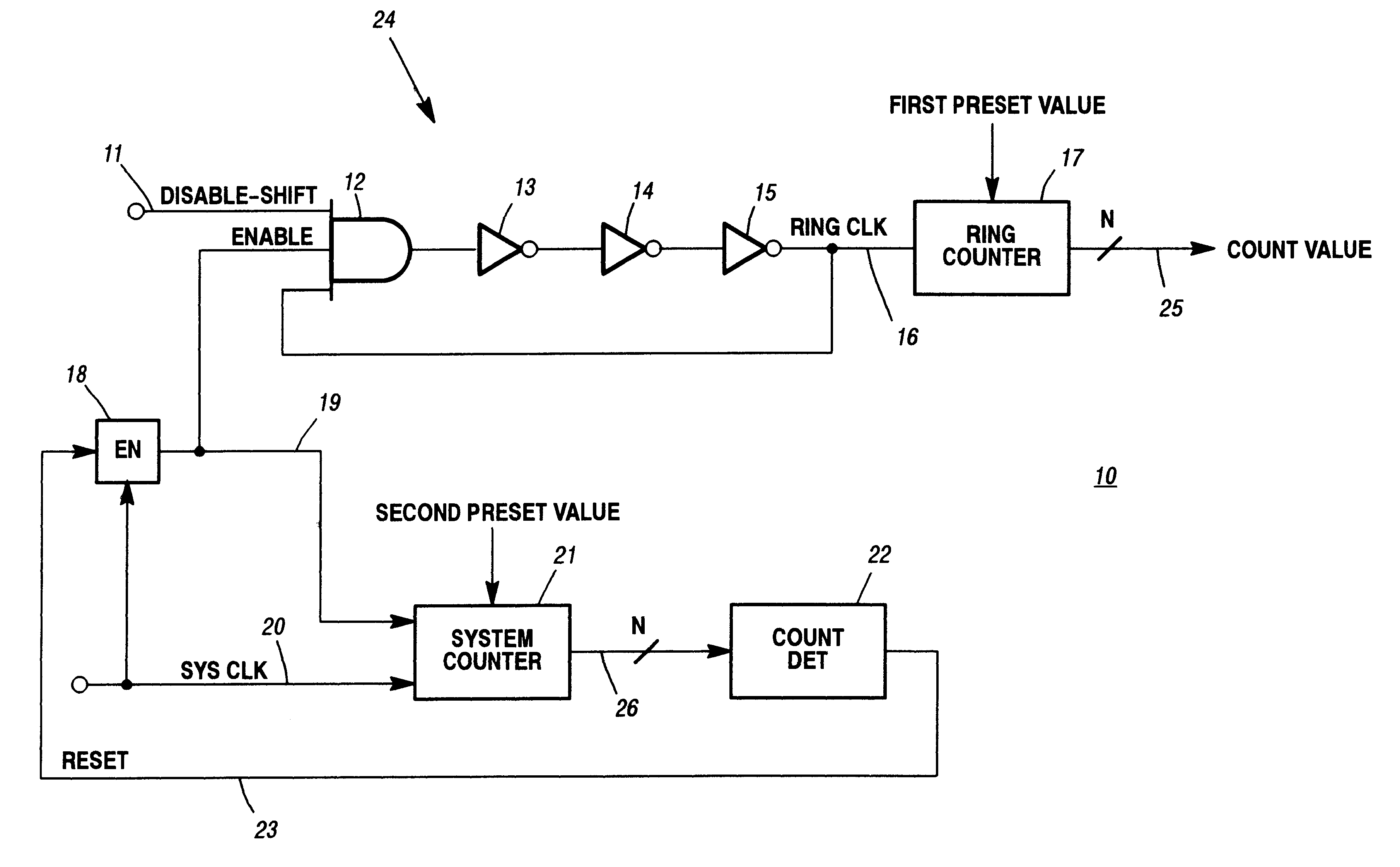
FIG. 1 is a system for measuring speed (frequency) of a ring oscillator in accordance with an exemplary embodiment of an aspect of the invention;
FIG. 2 is an exemplary embodiment of an enable circuit shown in FIG. 1 in accordance with an aspect of the invention;
FIG. 3 is an exemplary embodiment of a counter shown in FIG. 1 in accordance with an aspect of the invention;
FIG. 4 is an exemplary embodiment of a register coupled to a maintenance test set for statically shifting in and shifting out a test vector value in accordance with an embodiment of the invention;
FIG. 5 is an exemplary embodiment of a count detector shown in FIG. 1 in accordance with an aspect of the invention;
FIG. 6 is a timing diagram of relationships among various signals generated in the system shown in FIG. 1 in accordance with an aspect of the invention;
FIG. 7 is a method of the invention for measuring speed (frequency) of a ring oscillator formed on a chip in accordance with an aspect of the invention;
FIG. 8 is an illustration (not to scale) of a chip having formed therein multiple systems for measuring the speed (frequency) of a ring oscillator; and
FIG. 9 is a conventional ring oscillator providing a clock output signal including periodic pulses.
DETAILED DESCRIPTION OF THE INVENTION
Preferred embodiments of this invention will now be described with reference to the figures. It should be appreciated that this invention is not limited to the exemplary embodiments selected for illustration in the figures. It should also be appreciated that variations and modifications to the exemplary embodiments may be made without departing from the spirit or scope of this invention.
Referring to FIG. 1 there is shown a system, generally designated as <b>10</b>, for determining speed (or frequency) of a ring oscillator. System <b>10</b> includes ring oscillator <b>24</b>, ring counter <b>17</b>, enable circuit <b>18</b>, system counter <b>21</b> and count detector <b>22</b>. Each is described below.
Ring oscillator <b>24</b> includes inverters <b>13</b>, <b>14</b> and <b>15</b> connected in series to form a closed loop with positive feedback. Although three inverters are shown in FIG. 1, it will be appreciated that ring oscillator <b>24</b> may include a different odd-number of inverting elements. Ring oscillator <b>24</b> provides a ring clock (RCLK) signal as an oscillating output signal on line <b>16</b>. The ring clock signal is fed back into AND-gate <b>12</b> to provide positive feedback for maintaining oscillation. Depending on signal propagation delays of AND-gate <b>12</b> and inverters <b>13</b>-<b>15</b>, the ring clock signal includes an oscillation frequency that is inversely proportional to the number of inverters in the loop.
It will be appreciated that the oscillation frequency (speed) of ring oscillator <b>24</b> may also depend on ambient temperature, voltage and fabrication variations, stress and age of the elements in the loop. Depending on these factors, the ring clock signal may have an oscillation frequency (and a period) that varies from a maximum value to a minimum value. The ring clock signal on line <b>16</b> may be provided as an input signal to ring counter <b>17</b>. As will be explained, ring counter <b>17</b> may be a decrement counter for providing a count down based on each period in the ring clock signal. Ring counter <b>17</b> may count down from a preset value, in response to each rising edge (for example) of a pulse in the ring clock signal.
Also included in ring oscillator <b>24</b> is AND-gate <b>12</b> which enables the ring oscillation. In the exemplary embodiment of FIG. 1, when the output value of AND-gate <b>12</b> is 1, the ring clock signal on line <b>16</b> continues to oscillate, thereby providing rising edge pulses for counting by ring counter <b>17</b>. The output value of AND-gate <b>12</b> is 1, of course, when the ring clock (RCLK) signal on line <b>12</b> is 1, the enable (EN) signal on line <b>19</b> is 1 and the disable-shift signal on line <b>11</b> is 1.
It will be appreciated that the disable-shift signal on line <b>11</b> may be provided by a maintenance test set (not shown) to prevent shifting test vectors or combinations of logic values, into the ASIC, during a time interval that system <b>10</b> is measuring the speed of ring oscillator <b>24</b>. The disable-shift signal may also be provided to disable counting during a time interval between the end of shifting and the enable (EN) signal transitioning to a high (1) value (explained below).
The enable (EN) signal on line <b>19</b> is provided by enable circuit <b>18</b>. In the exemplary embodiment of FIG. 1 when the enable signal is 1 (and the disable-shift signal on line <b>11</b> is 1) ring oscillator <b>24</b> is oscillating. When the enable signal is 0, on the other hand, ring oscillator <b>24</b> stops oscillating. Enable circuit <b>18</b> may be a D-type flip-flop as shown in FIG. <b>2</b>. The set/reset signal on line <b>23</b>, provided to the D-pin of EN flip-flop <b>18</b>, appears as an enable (EN) signal at the Q-pin of the flip-flop, in response to clocking operation of the system clock (SCLK) on line <b>20</b>. In operation, when the system clock transitions from a low value (0) to a high value (1) and the set/reset signal is a high value (1), the enable (EN) signal on line <b>19</b> transitions to a high value (1). When the system clock transitions from a low value to a high value and the set/reset signal is a low value, however, the enable signal transitions to a low value.
Returning to FIG. 1, the enable signal may also be provided to system counter <b>21</b> to enable the system counter to count each pulse of the system clock on line <b>20</b>. As will be explained, system counter <b>21</b> may be a decrement counter and may count down from a preset value in response to, for example, each rising edge of the system clock. The count value from system counter <b>21</b> may be provided to count detector <b>22</b>. Upon detecting a predetermined count value, for example, count value of 1 or 0 (preferably count value of 1), count detector <b>22</b> may provide a reset signal on line <b>23</b> to enable circuit <b>18</b>. The reset signal may be clocked-out from enable circuit <b>18</b> onto line <b>19</b> by the next system clock, thereby causing the enable signal on line <b>19</b> to transition to a low (0) value. Transition of the enable signal to a low value concurrently stops ring oscillator <b>24</b> and system counter <b>21</b>.
An exemplary embodiment of ring counter <b>17</b> and system counter <b>21</b> is illustrated in FIG. <b>3</b>. In general, there is shown decrement counter <b>30</b> including multiplexer <b>31</b>, register <b>32</b> and decrementer <b>33</b> connected in series. Register <b>32</b> is a N-bit register comprised of N number of D flip-flops (one shown). N-parallel bits of data are provided on the D-pins of the register and N-parallel bits of data are provided on the Q-pins of the register. The data is dynamically loaded into the register by clocking operation of the clock signal (system clock) on line <b>36</b>. Loading may be in response to the clock signal transitioning from a low (0) value to a high (1) value. The data output from the Q-pins includes a value of N-parallel bits, designated as count value, on line <b>34</b>.
Decrementer <b>33</b>, as shown, receives the current count value from register <b>32</b> and decrements the count value by one (1). The output value (Q−1) is fed back to the D<b>1</b>-pin of multiplexer <b>31</b>. The Z output data of multiplexer <b>31</b> is provided to the D-pins of register <b>32</b>. On a next transition of the clock, register <b>32</b> presents this new data value on the Q-pins. Decrementer <b>33</b>, in turn, decrements the data value by one (1), thus repeating the process. Multiplexer <b>31</b> provides output data values to register <b>32</b>, when the enable signal on line <b>35</b> is a high (1) value (for example).
As explained below, decrement counter <b>30</b> includes a preset data value shifted into register <b>32</b>. The preset data value is the starting count value from which decrement counter <b>30</b> begins the count down. The preset data value may be shifted into register <b>32</b> using static shifting via a maintenance test set. Static shifting may be used to load a known value into any or all flip-flops (for example) on a chip. Alternate sets of pins into the flip-flop may be used, such as shift clock (SHCLK), shift data in (SDI) and shift data out (SDO). The shift clock and shift data in pins of the flip-flop may be used during the static shifting mode. The clock (CLK) and D pins of the flip-flop may be used during the normal functional mode (static shifting mode disabled). The system clock at the CLK pin and the shift clock at the SHCLK pin may not be used at the same time, because the result may be indeterminate.
An example of register <b>40</b> including three D-flip-flops <b>41</b>, <b>42</b> and <b>43</b> connected to maintenance test set <b>44</b> is shown in FIG. <b>4</b>. It will be appreciated that although three flip-flops are shown in the figure, register <b>40</b> may include more than three flip-flops. Register <b>40</b>, as shown, is a 3-bit register which receives three functional parallel data bits on lines D<sub>1</sub>, D<sub>2 </sub>and D<sub>3</sub>, and outputs three functional parallel data bits on lines Q<sub>1</sub>, Q<sub>2 </sub>and Q<sub>3</sub>. Clocking in data on lines D<sub>1</sub>, D<sub>2 </sub>and D<sub>3 </sub>and clocking out data on lines Q<sub>1</sub>, Q<sub>2 </sub>and Q<sub>3 </sub>is controlled by a system clock, as previously described (dynamic loading). The system clock may be a clock residing on the chip or a clock residing in the maintenance test set. When the system clock is operating, the shift clock is not operating.
In the static shifting mode, the system clock is turned-off. Maintenance test set <b>44</b> may then shift data into the register via the shift data in (SDI) line that is coupled to flip-flop <b>41</b>, using the shift clock. In the example shown, three data values may be loaded into the three flip-flops, using the shift clock. Data may also be shifted out in the static shifting mode from the shift data out (SDO) line of flip-flop <b>43</b> using the same shift clock. It will be appreciated that the SDO line and the SDI line are at opposite ends of the shift chain and may be fed and received by maintenance test logic (not shown). As data is shifted out from these flip-flops, the data values may be read or recorded from the SDO line at the appropriate time.
It will also be appreciated that maintenance test set <b>44</b> may perform ASIC testing by shifting in an appropriate value (to test a particular area of logic on the chip), issue a test clock (via test logic control), and then shift out the new data value from the logic (flip-flops, for example). The new data value may be compared against an expected data value.
Returning to the description of FIG. 1, a first preset value may be shifted into ring counter <b>17</b> using the maintenance test set. The first preset value may be 2047, for example. It will be appreciated that an 11-bit counter (including a register having 11 flip-flops) has 2<sup>11 </sup>different values and may count down from 2047 (2048−1) to 0. In a similar manner, a second preset value may be shifted into system counter <b>21</b> using the maintenance test set. The second preset value may be 1023, for example. It will be appreciated that a 10-bit counter (including a register having 10 flip-flops) has 2<sup>10 </sup>different values and may count down from 1023 (1024−1) to 0.
The preset values and the bit size of each counter may be determined as follows. Ring counter <b>17</b> counts clocks (pulses) from ring oscillator <b>24</b> and system counter <b>21</b> counts clocks from the system clock. If both counters are concurrently enabled and if the ring oscillator period is close to the system clock period, then a similar number of ring counter clocks and system counter clocks may occur. In order to save on the amount of logic for making the ring oscillator, and since most chips are faster than a worst case chip specified by the manufacturer (perhaps 2 or 3 times faster), the period of the ring oscillator is made smaller than the period of the system clock. Therefore, if the system counter is made, for example, 10-bits wide (10-bit counter), then the ring counter may be made 12 or 13-bits wide (12 or 13-bit counter). In this manner, the ring counter may count down 2 or 3 times faster than the system counter, without the ring counter stopping prematurely at a 0 value.
In operation, after statically shifting a first preset value into ring counter <b>17</b> and a second preset value into system counter <b>21</b>, the system clock on line <b>20</b> may be turned on. Enable circuit <b>18</b> may then be dynamically shifted by the system clock to provide the enable signal on line <b>19</b>. In turn, ring oscillator <b>24</b> may begin to oscillate and provide the ring clock signal on line <b>16</b>. Ring counter <b>17</b> may begin to count down from the first preset value. Concurrently, system counter <b>21</b> may begin to count down from the second preset value.
The count value output on line <b>26</b> (also, for example, the count value output on line <b>34</b> in FIG. 3) may be received by count detector <b>22</b>, as shown in FIG. <b>1</b>. Count detector <b>22</b> may be set to detect a count value of 1 on line <b>26</b>. When detected, count detector <b>22</b> may provide a reset signal on line <b>23</b>. The enable circuit may be reset by the reset signal on the next transition of the system clock. This may cause the ring oscillator to stop oscillating and the ring counter to stop counting. The count value on line <b>25</b> may be statically shifted out from the ring counter to the test maintenance set.
An exemplary embodiment of count detector <b>22</b> is shown in FIG. <b>5</b>. As shown, detector <b>50</b> detects a count value of 1 and provides the reset signal in response to the detection. For discussion purpose, detector <b>50</b> includes inverters <b>51</b>, <b>52</b>, <b>54</b> and AND-gate <b>53</b>, configured as shown, and logically detects 3 bits (Q<sub>0</sub>, Q<sub>1 </sub>and Q<sub>2 </sub>of a register) having a value of 1.
The operation of system <b>10</b> (FIG. 1) is further explained with reference to the timing diagram shown in FIG. <b>6</b>. As shown, SCLK is the system clock signal on line <b>20</b>. EN is the enable signal on line <b>19</b>. RCLK is the ring clock signal on line <b>16</b>. System counter (SYSCOUNT) <b>21</b> begins to count down from a preset value of 1023 (for illustration purpose assumed to be a 10-bit counter). Ring counter (RING COUNT) <b>17</b> begins to count down from a preset value of 2047 (for illustration purpose assumed to be an 11-bit counter).
As shown in FIG. 6, at time t<sub>1</sub>, SCLK causes EN to transition to a 1 value. SYSCOUNT, which is enabled by EN, begins a count down from 1023 in response to each positive transition of SCLK. EN transitioning to a 1 value also causes RCLK to be enabled. RINGCOUNT begins to count down from 2047 in response to each positive transition of RCLK.
At time t<sub>2</sub>, the count detector detects a value of 1 from SYSCOUNT and resets EN (on the next clock of SCLK). In turn, RCLK stops oscillating and RINGCOUNT stops at a count of 72 (for example). The count value of 72 (for example) may be shifted out to the maintenance test set via line <b>25</b>.
The ring oscillator speed may be determined from the following equation: <maths><math><mrow><mrow><mi>ring</mi><mo></mo><mstyle><mtext> </mtext></mstyle><mo></mo><mrow><mi>osc</mi><mo>.</mo><mstyle><mtext> </mtext></mstyle><mo></mo><mi>frequency</mi></mrow></mrow><mo>=</mo><mrow><mfrac><mrow><mi>Ring</mi><mo></mo><mstyle><mtext> </mtext></mstyle><mo></mo><mi>Count</mi><mo></mo><mstyle><mtext> </mtext></mstyle><mo></mo><mi>down</mi></mrow><mrow><mi>System</mi><mo></mo><mstyle><mtext> </mtext></mstyle><mo></mo><mi>Count</mi><mo></mo><mstyle><mtext> </mtext></mstyle><mo></mo><mi>down</mi></mrow></mfrac><mo>×</mo><mi>system</mi><mo></mo><mstyle><mtext> </mtext></mstyle><mo></mo><mi>frequency</mi></mrow></mrow></math><img id="EMI-M00001" file="US06657504-20031202-M00001.TIF" img-content="math" img-format="tif" alt="embedded image" /><attachments><attachment idref="MATHEMATICA-00001" attachment-type="nb" file="US06657504-20031202-M00001.NB" /></attachments></maths>
In the example shown in FIG. 6, system frequency of SCLK is assumed to be 100 MHz (the value may be based on the worst case timing analysis of the chip). The ring oscillator frequency of RCLK may be computed from the above equation, as follows: <maths><math><mrow><mrow><mi>RCLK</mi><mo></mo><mstyle><mtext> </mtext></mstyle><mo></mo><mi>frequency</mi></mrow><mo>=</mo><mrow><mrow><mn>100</mn><mo></mo><mstyle><mtext> </mtext></mstyle><mo></mo><mi>MHz</mi><mo>×</mo><mfrac><mrow><mn>2047</mn><mo>-</mo><mn>72</mn></mrow><mn>1023</mn></mfrac></mrow><mo>=</mo><mrow><mn>193</mn><mo></mo><mstyle><mtext> </mtext></mstyle><mo></mo><mrow><mi>MHz</mi><mo>.</mo></mrow></mrow></mrow></mrow></math><img id="EMI-M00002" file="US06657504-20031202-M00002.TIF" img-content="math" img-format="tif" alt="embedded image" /><attachments><attachment idref="MATHEMATICA-00002" attachment-type="nb" file="US06657504-20031202-M00002.NB" /></attachments></maths>
Thus, in the above example, the chip (on which system <b>10</b> resides) is running at approximately twice the speed that a worst case analysis predicts.
Referring to FIG. 7, there is shown a method of determining speed (frequency) of a ring oscillator on an ASIC or other chip. The method, generally designated as <b>70</b>, starts in step <b>71</b> and proceeds to set the enable (EN) circuit (for example EN <b>18</b> in FIG. 1) to a 0 value. A first preset value is shifted (step <b>73</b>) into the ring counter residing on the chip (for example ring counter <b>17</b>). A second preset value is shifted (step <b>74</b>) into the system counter residing on the chip (for example system counter <b>21</b>). These values may be statically shifted into the counters, for example, by using maintenance test set <b>44</b> of FIG. <b>4</b>.
Step <b>75</b> turns on the system clock and the enable circuit is dynamically shifted to a 1 value in step <b>76</b>. The system clock may be a clock signal generated by maintenance test set <b>44</b> and may be set to a predetermined frequency.
The system counter begins to count down in response to system clock pulses (step <b>77</b>). When detecting a predetermined count value (for example a value of 1), step <b>77</b> resets the enable circuit. The ring oscillator is stopped and the ring counter, in turn, stops counting down because the ring clock pulses have stopped.
Step <b>78</b> turns off the system clock. Next, in step <b>79</b>, the ring counter value may be statically shifted out from the register of the ring counter. The ring oscillator frequency may next be computed (step <b>80</b>) using the equation described previously. The method ends in step <b>81</b>.
FIG. 8 is an exemplary embodiment of chip <b>85</b> which may be an ASIC. Logic circuits may be formed on chip <b>85</b> using a hardware description language (HDL). The HDL may be synthesized into logic gates and may be automatically arranged in a layout to form the ASIC's physical design. In the example shown, four systems <b>10</b>, each measuring speed (frequency) of a ring oscillator, are formed at respective corners of the chip.
Although illustrated and described herein with reference to certain specific embodiments, the present invention is nevertheless not intended to be limited to the details shown. Rather, various modifications may be made in the details within the scope and range of equivalents of the claims and without departing from the spirit of the invention.
Contents5
10 sheets
Sheet 1 Sheet 2 Sheet 3 Sheet 4 Sheet 5 Sheet 6 Sheet 7 Sheet 8 Sheet 9 Sheet 10
Every citation, both ways
| Document | Relation | Office | Cited during |
|---|---|---|---|
| US2008144407A1 | Cited by | United States of America | Pre-grant |
| US7592842B2 | Cited by | United States of America | Applicant |
| US9830889B2 | Cited by | United States of America | Applicant |
| US9490817B1 | Cited by | United States of America | Applicant |
| US2009079460A1 | Cited by | United States of America | Pre-grant |
| US8102190B2 | Cited by | United States of America | Applicant |
| US2009002081A1 | Cited by | United States of America | Pre-grant |
| US8786374B2 | Cited by | United States of America | Search report |
| US7893776B1 | Cited by | United States of America | Applicant |
| US7714670B1 | Cited by | United States of America | Applicant |
| US2005149777A1 | Cited by | United States of America | Pre-grant |
| US9106233B1 | Cited by | United States of America | Applicant |
| US7414485B1 | Cited by | United States of America | Applicant |
| US7646228B1 | Cited by | United States of America | Applicant |
| US2004263192A1 | Cited by | United States of America | Pre-grant |
| US7705633B2 | Cited by | United States of America | Applicant |
| US8624680B2 | Cited by | United States of America | Applicant |
| US7889014B1 | Cited by | United States of America | Applicant |
| US7595664B1 | Cited by | United States of America | Applicant |
| US7667478B2 | Cited by | United States of America | Applicant |
| US8451025B2 | Cited by | United States of America | Applicant |
| US2009212815A1 | Cited by | United States of America | Pre-grant |
| US7193427B2 | Cited by | United States of America | Search report |
| US7724025B2 | Cited by | United States of America | Applicant |
| US7394681B1 | Cited by | United States of America | Applicant |
| US8018252B2 | Cited by | United States of America | Applicant |
| US7868638B2 | Cited by | United States of America | Applicant |
| US9088288B1 | Cited by | United States of America | Applicant |
| US7710160B2 | Cited by | United States of America | Applicant |
| US7739531B1 | Cited by | United States of America | Applicant |
| US7746183B2 | Cited by | United States of America | Search report |
| US8354857B1 | Cited by | United States of America | Search report |
| US7872492B2 | Cited by | United States of America | Applicant |
| US2012274408A1 | Cited by | United States of America | Pre-grant |
| US2010169045A1 | Cited by | United States of America | Pre-grant |
| US2010060306A1 | Cited by | United States of America | Pre-grant |
| US7724016B2 | Cited by | United States of America | Applicant |
| US9595968B2 | Cited by | United States of America | Applicant |
| US7626409B1 | Cited by | United States of America | Applicant |
| US6885210B1 | Cited by | United States of America | Search report |
| US2014022022A1 | Cited by | United States of America | Pre-grant |
| US7889013B2 | Cited by | United States of America | Search report |
| US9584136B1 | Cited by | United States of America | Applicant |
| US7642866B1 | Cited by | United States of America | Applicant |
| US7671621B2 | Cited by | United States of America | Applicant |
| US2008106295A1 | Cited by | United States of America | Pre-grant |
| US2009250698A1 | Cited by | United States of America | Pre-grant |
| US7315178B1 | Cited by | United States of America | Applicant |
| US7710153B1 | Cited by | United States of America | Applicant |
| US2006181325A1 | Cited by | United States of America | Pre-grant |
| US10747258B1 | Cited by | United States of America | Search report |
| US9973331B1 | Cited by | United States of America | Applicant |
| US2004263200A1 | Cited by | United States of America | Pre-grant |
| US9372948B1 | Cited by | United States of America | Search report |
| US10432174B2 | Cited by | United States of America | Applicant |
| US2009121737A1 | Cited by | United States of America | Pre-grant |
| US2006267618A1 | Cited by | United States of America | Pre-grant |
| US7495466B1 | Cited by | United States of America | Applicant |
| US7768295B2 | Cited by | United States of America | Applicant |
| US7109734B2 | Cited by | United States of America | Search report |
| US7652507B1 | Cited by | United States of America | Applicant |
| US7358755B1 | Cited by | United States of America | Search report |
| US7679949B1 | Cited by | United States of America | Applicant |
| US6933739B1 | Cited by | United States of America | Search report |
| US2009177442A1 | Cited by | United States of America | Pre-grant |
| US2007008012A1 | Cited by | United States of America | Pre-grant |
| US7592839B2 | Cited by | United States of America | Applicant |
| US7489152B2 | Cited by | United States of America | Applicant |
| US2008143372A1 | Cited by | United States of America | Pre-grant |
| US8315830B2 | Cited by | United States of America | Search report |
| US7663408B2 | Cited by | United States of America | Applicant |
| US7768356B2 | Cited by | United States of America | Applicant |
| US2010102842A1 | Cited by | United States of America | Pre-grant |
| US2009058540A1 | Cited by | United States of America | Pre-grant |
| US9178505B2 | Cited by | United States of America | Applicant |
| US8421506B2 | Cited by | United States of America | Search report |
| US7635992B1 | Cited by | United States of America | Applicant |
| US7456628B2 | Cited by | United States of America | Applicant |
| US8022731B2 | Cited by | United States of America | Applicant |
| US8008957B2 | Cited by | United States of America | Applicant |
| US2011291742A1 | Cited by | United States of America | Pre-grant |
| US10747258B1 | Cited by | United States of America | Search report |
| US7348857B1 | Cited by | United States of America | Search report |
| JP40108465A | Cites | Japan | Search report |
| US4697140A | Cites | United States of America | Search report |
| US4758821A | Cites | United States of America | Search report |
| US5045811A | Cites | United States of America | Search report |
| US5087842A | Cites | United States of America | Search report |
| US5097208A | Cites | United States of America | Search report |
| US5099196A | Cites | United States of America | Search report |
| US5331294A | Cites | United States of America | Search report |
| US5448202A | Cites | United States of America | Search report |
| US5457400A | Cites | United States of America | Search report |
| US5619463A | Cites | United States of America | Search report |
| US5818250A | Cites | United States of America | Search report |
1 member in 1 office
Priority claims2
| Document | Office | Kind | Date |
|---|---|---|---|
| 13554202 | United States of America | A | |
| US20020135542 | – | – | – |
Members1
| Document | Office | Kind | |
|---|---|---|---|
| US6657504B1This record | United States of America | B1 |
25 transactions on the USPTO file
Allowed without a rejection on record.
- Non-final rejections
- 0
- Final rejections
- 0
- RCEs
- 0
- Appeals
- 0
Over time
Point at a mark for the transactionTransactions
| Event | Code | |
|---|---|---|
| Recordation of Patent Grant MailedPGM/ | PGM/ | |
| Patent Issue Date Used in PTA CalculationAllowedPTAC | PTAC | |
| Issue Notification MailedAllowedWPIR | WPIR | |
| Receipt into PubsR1021 | R1021 | |
| Application Is Considered Ready for IssuePILS | PILS | |
| Issue Fee Payment VerifiedN084 | N084 | |
| Issue Fee Payment ReceivedIFEE | IFEE | |
| Receipt into PubsR1021 | R1021 | |
| Workflow - File Sent to ContractorSENT | SENT | |
| Receipt into PubsR1021 | R1021 | |
| Dispatch to PublicationsD1220 | D1220 | |
| Mail Notice of AllowanceAllowedMN/=. | MN/=. | |
| Notice of Allowance Data Verification CompletedAllowedN/=. | N/=. | |
| Case Docketed to Examiner in GAUDOCK | DOCK | |
| Case Docketed to Examiner in GAUDOCK | DOCK | |
| Application Dispatched from OIPEOIPE | OIPE | |
| Application Is Now CompleteCOMP | COMP | |
| Workflow - Drawings FinishedDRWF | DRWF | |
| Workflow - Drawings Matched with File at ContractorDRWM | DRWM | |
| Additional Application Filing FeesADDFLFEE | ADDFLFEE | |
| A statement by one or more inventors satisfying the requirement under 35 USC 115, Oath of the ApplicOATHDECL | OATHDECL | |
| Applicant has submitted new drawings to correct Corrected Papers problemsCORRDRW | CORRDRW | |
| Notice Mailed--Application Incomplete--Filing Date AssignedINCD | INCD | |
| IFW Scan & PACR Auto Security Review | – | |
| Initial Exam Team nnIEXX | IEXX |
24 legal events, as the office reported them to INPADOC
Over the term
Point at a mark for the eventEvents
| Event | Code | |
|---|---|---|
| AssignmentAS | AS | |
| AssignmentAS | AS | |
| AssignmentAS | AS | |
| AssignmentAS | AS | |
| AssignmentAS | AS | |
| AssignmentAS | AS | |
| Fee paymentFPAY | FPAY | |
| AssignmentAS | AS | |
| AssignmentAS | AS | |
| AssignmentAS | AS | |
| Fee paymentFPAY | FPAY | |
| AssignmentAS | AS | |
| AssignmentAS | AS | |
| AssignmentAS | AS | |
| AssignmentAS | AS | |
| AssignmentAS | AS | |
| AssignmentAS | AS | |
| AssignmentAS | AS | |
| AssignmentAS | AS | |
| AssignmentAS | AS | |
| AssignmentAS | AS | |
| Fee paymentFPAY | FPAY | |
| Information on status: patent grantGrantedPATENTED CASESTCF | STCF | |
| AssignmentAS | AS |
Numbers
- Publication, DOCDB
- 6657504
- Publication, EPODOC
- US6657504
- Application
- 10135542
- Application, DOCDB
- 13554202
- Application, EPODOC
- US20020135542
Titles
- English
- System and method of determining ring oscillator speed
Patent term adjustment
- A delay
- +9 daysthe office missed an examination deadline
- Net adjustment
- 9 days
Classification
- CPC, 1
- G01R31/2824
- IPC, 1
- G01R31 28
- USPC, 2
- 331057000
- 324762020