Multi-band narrow frequency band wireless receiver for automobile data
Abstract
[Task] Provided is a multi-band universal receiver capable of transmitting from a transmitter of various frequency bands.
Solution.It includes an antenna circuit (1-4) connected to a unit (10-15) that processes carriers of a plurality of specific frequency bands modulated by a data signal. The unit (10-15) includes a frequency transposition circuit (11, 23-28) connected to a demodulation circuit (13) that supplies data to be demolished, and a frequency discrimination circuit (21, 22) is an antenna. Connected to the circuit (1-4), each reception level in the above band is determined in order to compare the received signal levels with each other and control the frequency shift circuit (11, 23-28) according to the comparison result. ..
Term
Term ended
Projected expiry passed 2 May 2021, 5.4 years ago.
- Priority
- Filed
- Published
- Projected expiry
- Today
8 claims: 1 independent, 7 dependent
- 1【特許請求の範囲】 【請求項1】データ信号により変調された特定周波数バンドの受信搬送波を処理するユニット(10-15)に接続されたアンテナ手段(1-4)を具備しており、 前記ユニット(10-15)が、前記搬送波の周波数の移調を行う手段(11、23-28)を具備しており、この手段は前記移調された搬送波を復調する手段(13)に接続されており、復調手段は前記被復調データを供給するように構成されており、 前記アンテナ手段(1-4)が、複数の周波数バンドを受信できるように構成され、周波数弁別手段(21、22)が、前記アンテナ手段(1-4)に接続され、前記バンド内の各受信レベルを相互に比較しその比較結果に応じて前記周波数移調手段(11、23-28)を制御するために、前記バンド内の各受信レベルを決定するように構成されていることを特徴とする自動車データ用の狭周波数帯域無線受信機。
- 2【請求項2】請求項1記載の自動車データ用の狭周波数帯域無線受信機であって、 前記周波数移調手段が、マスタオシレータ(23)に対するスレーブオシレータ(27)のスレーブループ(24-27)を具備することを特徴とする自動車データ用の狭周波数帯域無線受信機。
- 3【請求項3】請求項2記載の自動車データ用の狭周波数帯域無線受信機であって、 前記スレーブループ(24-27)が、2つの各入力により前記2つのオシレータ(23、27)に接続された位相比較器(24)を具備するとともに、前記入力の一方に挿置されており、かつ前記弁別手段(21、22)により制御されるように構成された調節可能な周波数変更回路(25)を備えていることを特徴とする自動車データ用の狭周波数帯域無線受信機。
- 4【請求項4】請求項2記載の自動車データ用の狭周波数帯域無線受信機であって、 前記ループ(24-27)が、前記弁別手段(21、22)により制御されるように構成された周波数除算器(28)を介して前記受信信号の周波数を移調するミクサ(11)を制御することを特徴とする自動車データ用の狭周波数帯域無線受信機。
- 5【請求項5】請求項2記載の自動車データ用の狭周波数帯域無線受信機であって、 前記マスタオシレータ(23)が、前記弁別手段(21、22)によりその周波数が制御されるように構成されたものであることを特徴とする自動車データ用の狭周波数帯域無線受信機。
- 6【請求項6】請求項1記載の自動車データ用の狭周波数帯域無線受信機であって、 前記弁別手段(21、22)が、前記周波数バンドを選択する比較器(213)の入力に接続された2つの周波数シフトバンドパスフィルタ(211、212)を具備することを特徴とする自動車データ用の狭周波数帯域無線受信機。
- 7【請求項7】請求項6記載の自動車データ用の狭周波数帯域無線受信機であって、 前記比較器(213)が、その入力において、2つの雑音除去しきい値回路を具備することを特徴とする自動車データ用の狭周波数帯域無線受信機。
- 8【請求項8】請求項7記載の自動車データ用の狭周波数帯域無線受信機であって、 前記比較器(213)が、その入力の一方を他方入力よりも安定して優先させる回路を具備することを特徴とする自動車データ用の狭周波数帯域無線受信機。
Independent claims8
67 paragraphs in 1 section, as filed
Description: TECHNICAL FIELD [Detailed description of the invention]
【0001】
[Technical field to which the invention belongs]
The present invention relates to a short range radio receiver that is installed in an automobile and receives data such as a remote control signal for locking and unlocking a door, for example.
【0002】
[Conventional technology]
Conventional receivers for such remote control signals operate in a single frequency band of about 434MHz in France and about 315MHz in the United States and Japan.
【0003】
[Problems to be Solved by the Invention]
Due to such a natural frequency band in a particular country, interference often occurs between portable remote control transmitters of vehicles parked in the same parking lot.
【0004】
On the other side, at a global level, manufacturers of these receivers must design transmitters according to the requirements of car manufacturers, that is, in a limited production process that is even more costly. Also note the fact that another frequency band of about 868MHz is currently allowed in Europe.
【0005】
Therefore, Applicants provide a multi-band universal receiver capable of transmitting from transmitters of various frequency bands.
【0006】
[Means for solving problems]
To this end, the present invention relates to a narrow frequency band radio receiver for automotive data, comprising antenna means connected to a unit that processes a received carrier of a specific frequency band modulated by a data signal. The unit is equipped with means for performing frequency transposition of the carrier wave, which means is connected to a means for demodulating the transposed carrier wave, and the demodulating means is configured to supply data to be demodulated. Has been done. Further, in the present receiver, the antenna means is configured to receive a plurality of frequency bands, and the frequency discrimination means is connected to the antenna means to compare the reception levels within the range of the frequency band with each other. It is characterized in that it is configured to determine each reception level within the range of the frequency band in order to control the frequency transposition means according to the comparison result.
【0007】
Therefore, this receiver can receive only signals of one frequency band of a plurality of frequency bands, and the frequency band having the maximum energy becomes the actual effective frequency band.
【0008】
BEST MODE FOR CARRYING OUT THE INVENTION
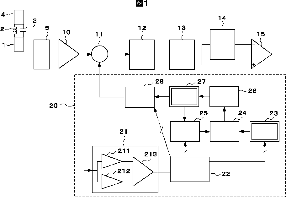
The present invention will be better understood by utilizing the following description relating to a preferred embodiment of the receiver of the present invention and by referring to FIG. 1, which schematically shows the circuit of the receiver of the present invention. Let's go.
【0009】
The multi-band receiver shown in FIG. 1 is a 2-band receiver in this embodiment and includes an antenna that receives a carrier wave modulated with binary data, and this antenna is a 1/4 wavelength wave of the 868 MHz band. It is formed by a radiating element 1 tuned to, and an electrically equivalent element (idetical) through a tuning circuit LC in which an inductance 2 and a capacitor 3 connected in parallel are tuned to the 868 MHz band. element) Connected to 4. In this assembly, a resonant antenna tuned to 434MHz and 868MHz is constructed. Element 1 is connected to the input of a bandpass filter 5 with two bands centered around 434MHz and 868MHz to control the low noise amplifier 10. At the output of amplifier 10, there is a frequency-shifting mixer, or frequency-shifting mixer 11, that in this case supplies a carrier signal transposed to a fixed intermediate frequency of 10.7 MHz, and this fixed intermediate frequency passes through the bandpass filter 12. Further, it passes through the non-inverting input of the amplitude comparator 15 and the demodulator 13 that gives demodulated data to the inverting input of the comparator 15, that is, the negative input via the integrator circuit 14. The integrating circuit 14 provides a reference threshold, that is, approximately half of the peak value (bit = 1) of the signal to be demodulated stored in the circuit 14. Therefore, the comparator 15 provides a received signal with bit = 0 or bit = 1.
【0010】
Mixer 11 should select one of the frequency bands that can be efficiently received by antennas 1 to 4, namely 868MHz (then element 4 is separated by the tuning circuit LC), or half that frequency, 434MHz. Controlled by the present invention, circuits LC2, 3 become receivable for this frequency, and elements 1 and 4 are equivalent to a single element tuned to a 1/4 wavelength wave of 434MHz.
【0011】
The mixer 11 that supplies the intermediate frequency signal is controlled by an assembly consisting of circuits 21-28 as a whole referenced in 20.
【0012】
To this end, the output of the amplifier 10 is connected to a frequency band selection circuit, or frequency discrimination circuit 21, comprising two types of circuits 211 and 212, each of which has two types of circuits 211 and 212. It is tuned to the band of, and individually supplies a rectified integral signal with the radio energy level received in the band involved. Therefore, circuits 211 and 212 are frequency shift bandpass filters, followed by a rectifier and an integrator.
【0013】
The comparator 213 compares the amplitudes of the two levels of signals described above, provides the corresponding bit signal to the microprocessor 22, and thus specifies the effective band that provides the maximum energy.
【0014】
The microprocessor 22 controls the operation of the frequency generators 23-28 that form the local oscillator, and controls the frequency according to the output of the comparator 213 and thus the effective band.
【0015】
The local frequency generator is connected via the loop bandpass filter 26 to the first input of the phase comparator 24, which controls the frequency adjustment of the variable frequency slave oscillator 27 (in this case, controlled by the voltage (VCO)). The stable master oscillator 23 is provided, and the output of the slave oscillator 27 is returned to the second input of the phase comparator 24 via the frequency divider by the factor M referred to in 25. The output of VCO27 controls mixer 11 via a factor N divider referenced in 28.
【0016】
In this embodiment, the microprocessor 22 uses the dividers 25 and 28, as well as the variable frequency oscillator 23, to control or adjust the frequencies of the frequency generators 23-28. In another embodiment, it is possible to provide only one of these three control means.
【0017】
The dividers 25 and 28, respectively, are formed from one or more counters that form a clock and count the period of the signal generated in the upstream circuit. These counters provide consecutively identical patterns of different counting states, each pattern consisting of a specific number of variable states. Therefore, the divider counter in question counts in a variable length loop and divides the change-of-state pulse for dividing the downstream stage by 2 for each of the decoded loop specific states. Provided for output from vessel 25 or 28. Therefore, in the downstream stage of dividing by 2, an alternative is to provide a signal with a value of 0 during one pass through the loop and a signal with a value of 1 of the same duration during the next pass. To do. As a result, this signal has a form factor of 0.5, so its energy spectrum is essentially centered on the basic frequency that allows the Mixer 11 to operate at good output. become.
【0018】
In this embodiment, the loop length adjustment, which determines the values M and N, causes the "all set" state of a series of counters connected in order upon arrival of the next clock signal in the upstream circuit. It is executed by decoding and putting the counter in the initial state determined by the microprocessor 22, and does not naturally bring that state into an "all reset" state. The number of states thus set from the initial state to the final all set state is the desired value M during time regeneration, up to factor 2 near the output divider stage. Or matches N. Such pre-placement is individually controlled by specific bits of the microprocessor 22 and is an individual parallel input that is all unlocked in an "all set" state. This is done by setting the desired basic stage of the counter with a gate.
【0019】
Next, the operation of the receiver will be described in more detail.
【0020】
The operation of the main chain network consisting of circuits 5 and 10 to 15 is standard and well known and does not need further explanation.
【0021】
The selection circuit 21 operates continuously or periodically to control the microprocessor 22 and the mixer 11 without significant delay to provide an active signal to the downstream stages 12-15.
【0022】
When the radio wave is received in one of a plurality of bands, this band is identified by comparing each level of the two band signals from the circuits 211 and 212 by the comparator 213, and the identified band is micro. Notified to processor 22. In this case, it is premised that it is impossible to receive active signals of two types of bands at the same time. In order to prevent noise from one band that stably exceeds the effective signal level of the other band, which is inferior in detection sensitivity, it is appropriate for the purpose of comparing reception levels, for example, to equalize the two detection sensitivities. It is preferable to consider the sensitivity ratio of each of the two types of bands by proportionally amplifying and attenuating the output signal of circuit 211 or 212.
【0023】
The VCO27 oscillates at a frequency M times higher than the frequency of the oscillator 23 and therefore operates under favorable conditions. The VCO27 also provides the mixer 11 with a frequency N times lower than its own frequency. This frequency shows a difference of 10.7 MHz in this embodiment relating to the antenna carrier where transposition to the intermediate frequency is desired as described above. Therefore, the output frequency of local oscillators 23-28 should be 868 ± 10.7 = 857.3MHz or 878.7MHz for the high frequency band, or 434MHz lower than the above case for the low frequency band, 423.3MHz or 444.7MHz. is there.
【0024】
To pass from one of the frequencies in the high frequency band to one of the frequencies in the low frequency band, and vice versa, in microprocessor 22, for example, changing the coefficient M or N by factor 2 or almost 2 leaves the rest. The change is made according to this adjustment by changing the coefficient N or M. It will be found that the larger numbers of M and N allow for more precise adjustment. The oscillator 23 can also be adjusted, but since the oscillator has a good selection level at which the frequency is always stable, the adjustment is within a limited range in this case.
【0025】
In one variant, the divider 25 inserted on the input of the comparator 24 is connected to the VCO 27 and can be replaced with a rank M multiplier inserted on the inverse input. In either case, the divider 25 or the inverse equivalence multiplier causes a frequency change, tuning the slave oscillator 27 according to the frequency of the master oscillator 23.
【0026】
Corresponds to each of the two signals at the input of the comparator 213 and the sensitivity in each band in order to prevent unnecessary switching due to the noise of the comparator 213 when there is no active signal in the antennas 1 to 4. If neither of the two signals exceeds the corresponding low threshold, lock the comparator 213 to a predetermined state, or in the absence of a valid signal, that part. A threshold circuit may be provided with an additional dual comparator that transmits a signal to the microprocessor 22 in order to prohibit new commands for. In one variant, the comparator 213 itself acts as a defense against this noise, so each of its inputs is from two levels of signals received from circuits 211, 212 to achieve this goal. A threshold circuit for removing a constant voltage level is provided. As a modification, this threshold circuit may be provided in the above-mentioned circuits 211 and 212.
【0027】
To handle the case where there are no external commands on the two inputs due to the lack of an active signal and the threshold circuit that removes noise, the comparator 213 is therefore preferably of the two inputs. It is equipped with a circuit for at-rest priority polarisation (a circuit for at-rest priority polarisation), so that the high feedback resistance of the positive voltage that provides the internal low level command prevents the occurrence of output vibration. As a result, this input takes precedence over the other in the absence of external commands. This internal command becomes invalid when a valid external signal appears on the other input and exits the at-rest state.
【0028】
[Effect of the invention]
As described above, according to the present invention, it is possible to provide a multi-band universal receiver capable of transmitting from a transmitter of various frequency bands.
[Simple explanation of drawings]
[Figure 1]
It is a figure which shows schematic the circuit of the receiver of this invention.
[Explanation of symbols]
1 Radiant element 2 Inductance 3 Capacitor 4 An element that is electrically equivalent to the radiant element 1 5 bandpass filter 10 Low noise amplifier 11 Mixer 12 bandpass filter 13 Demodulator 14 Integrator circuit 15 Amplitude comparator 21 frequency band selection circuit 22 microprocessor 23 Master Oscillator 24 Phase comparator 25 divider 26 Bandpass filter 27 Slave oscillator 28 Divider 211 Frequency shift bandpass filter 212 Frequency shift bandpass filter 213 Comparator
3 sheets
Sheet 1 Sheet 2 Sheet 3
Every citation, both ways
| Document | Relation | Office | Cited during |
|---|---|---|---|
| JP2002064365A | Cites | Japan | Search report |
| JPH0312542U | Cites | Japan | Examiner |
| JPH0514427A | Cites | Japan | Search report |
| JPH07147529A | Cites | Japan | Search report |
| JPH11355169A | Cites | Japan | Search report |
10 members in 6 offices
Priority claims5
| Document | Office | Kind | Date |
|---|---|---|---|
| 0005689 | France | A | |
| 0005689 | France | A | |
| 0005689 | France | – | |
| 2000200005689 | – | – | – |
| FR20000005689 | – | – | – |
Members10
| Document | Office | Kind | |
|---|---|---|---|
| US2001039185A1 | United States of America | A1 | |
| FR2808633A1 | France | A1 | |
| EP1154582A1 | European Patent Office (EPO) | A1 | |
| JP2002009646AThis record | Japan | A | |
| FR2808633B1 | France | B1 | |
| US6965757B2 | United States of America | B2 | |
| EP1154582B1 | European Patent Office (EPO) | B1 | |
| DE60117739D1 | Germany | D1 | |
| DE60117739T2 | Germany | T2 | |
| ES2261360T3 | Spain | T3 |
11 legal events, as the office reported them to INPADOC
Over the term
Point at a mark for the eventEvents
| Event | Code | |
|---|---|---|
| Decision of refusalJAPANESE INTERMEDIATE CODE: A02A02 | A02 | |
| Notification of reasons for refusalJAPANESE INTERMEDIATE CODE: A131A131 | A131 | |
| Report on retrievalJAPANESE INTERMEDIATE CODE: A971007A977 | A977 | |
| Notification of resignation of power of attorneyJAPANESE INTERMEDIATE CODE: A7424RD04 | RD04 | |
| Written amendmentJAPANESE INTERMEDIATE CODE: A821A521 | A521 | |
| Notification of acceptance of power of attorneyJAPANESE INTERMEDIATE CODE: A7422RD02 | RD02 | |
| Written amendmentJAPANESE INTERMEDIATE CODE: A821A521 | A521 | |
| Written amendmentJAPANESE INTERMEDIATE CODE: A523A521 | A521 | |
| Written amendmentJAPANESE INTERMEDIATE CODE: A821A521 | A521 | |
| Written request for application examinationJAPANESE INTERMEDIATE CODE: A621A621 | A621 | |
| Notification of change in applicantJAPANESE INTERMEDIATE CODE: A711A711 | A711 |
Numbers
- Publication
- 2002-9646
- Publication, DOCDB
- 2002009646
- Publication, EPODOC
- JP2002009646
- Application
- 135062
- Application, DOCDB
- 2001135062
- Application, EPODOC
- JP20010135062
Titles2
- Japanese
- 自動車データ用のマルチバンド狭周波数帯域無線受信機
- English
- INDUSTRIAL APPLICABILITY: Multi-band narrow frequency band wireless receiver for automobile data
Classification
- CPC, 2
- H04B1/28
- H04B1/406
- IPC, 3
- H04B1 16
- H04B1 28
- H04B1 40